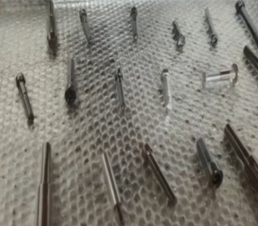
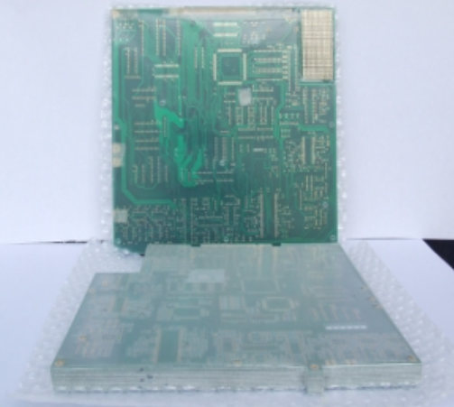
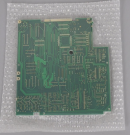
IDEAL-SA PCB skin pack film is special for PCB or clectronic Products skin packaging.
Using bubble wrap as the bottom film and SA film as the top film to achieve tight fitting packaging, in order to protect PCB or electronic products from damage.
IDEAL-SA PCB vacuum skin packaging film is designed for printed circuit boards, assembled circuit boards and selected electronic products that require secure positioning and visible packaging during handling and transportation.
The transparent top film is heated and vacuum formed around the product, then combined with a compatible bubble cushioning bottom film. This close-fitting packaging structure helps reduce movement, surface friction and handling damage while allowing the PCB or electronic assembly to remain visible without opening the package.
Standard 450 mm and 610 mm widths are available. Film thickness, roll weight and other specifications can be customized according to the PCB dimensions, component height, packaging machine and production requirements.
Width, thickness, roll weight and packaging specification
Documentation
RoHS and SGS documentation for applicable specifications
Sample Testing
Recommended before volume production
IDEAL-SA Film
Product
Standard Width
Thickness
Weight
SA
450mm,610mm
100um,12oum,150um,180um,200um,250um,300um ,350um
12.5-30kg/roll
Other Width and Thickness can be customized
Main features:
1.High transparency
2.High elongation to conform to the contours of product intimately
3.Excellent impact strength to protect from crude transport and handling.
4.Lower processing temperature to save energy and enhance efficiency.
5.No harmful fumes emit while packaging
6.Resistance to oil and grease
7.Products of all sizes and shapes can be packaged
8.Comply with RoHS and have SGS certification
Why Use PCB Vacuum Skin Packaging Film?
Secure Circuit Board Positioning
Vacuum forming draws the PCB skin packaging film closely around the circuit board and toward the cushioning bottom layer. This helps keep the board in its intended position and reduces movement inside the outer carton.
Protection During Handling and Transport
PCB boards and electronic assemblies may be exposed to vibration, repeated handling and stacking during storage and shipment. The close-fitting packaging structure helps reduce direct movement, surface contact and minor handling damage.
Clear Product Visibility
The transparent circuit board vacuum packaging film allows operators, warehouse personnel and customers to identify the PCB model, connectors and visible condition without opening the package.
Suitable for Different PCB Profiles
IDEAL-SA film can be selected for flat printed circuit boards as well as assemblies with raised connectors, capacitors, terminals and other components. Film thickness should be chosen according to the maximum product height, board weight and protruding component profile.
Custom Rolls for Existing Equipment
Film width, thickness and roll configuration can be adjusted according to the working width and unwinding requirements of the customer’s existing vacuum skin packaging machine.
Suitable PCB and Electronic Products
PCB vacuum skin packaging film can be considered for:
Bare printed circuit boards
Assembled PCB and PCBA products
Industrial control boards
Power supply boards
Communication circuit boards
LED control boards
Sensor and control modules
Electronic connector assemblies
Small electronic components
Repair and replacement circuit boards
Products with sharp solder joints, exposed pins or tall components should be evaluated through packaging trials before volume production.
For ordinary plastic parts, magnetic products and general hardware, our PE skin pack film may provide a more economical option.
How PCB Skin Packaging Works
A typical PCB skin packaging structure consists of the circuit board, a compatible bubble cushioning bottom film and the IDEAL-SA transparent top film.
During packaging:
The PCB or electronic assembly is positioned on the cushioning bottom material.
The PCB skin packaging film is heated to the appropriate forming condition.
Vacuum draws the film closely around the circuit board and raised components.
The top film combines with the compatible bottom material around the product.
The packaged PCB is cut or separated and prepared for outer-carton packing.
The final packaging result depends on the film thickness, PCB height, component profile, heating conditions, vacuum level and bottom material. Sample testing is therefore recommended before confirming a volume order.
How to Select the Right Film Specification
Selection Factor
Recommended Consideration
PCB Length and Width
Determine the required film and machine working width.
Maximum Component Height
Higher components require more film stretching during vacuum forming.
PCB Weight
Heavier boards may require a thicker film and stronger bottom structure.
Pins and Sharp Components
Protruding parts may require additional film thickness, protective covers or adjusted orientation.
Packaging Equipment
Confirm film width, core size and processing compatibility with the existing machine.
Shipping Conditions
Long-distance transportation may require stronger fixation and additional outer packaging.
Static Protection
Confirm whether the PCB or PCBA requires a controlled ESD packaging system.
The quickest way to identify the best solution for your needs is to speak with one of our team of
experts. We'll be able to quickly narrow down your options and give you objective advice on the best
fit.